Volunteers ( ESD Enthusiast)
Dr. Ajay
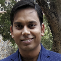 Dr. Ajay, was born and grew up in Bilaspur of Uttar Pradesh India . He obtained Ph.D. degree in Microelectronics, from University of Delhi, New Delhi, India in 2017. Thesis entitled “Modeling and Simulation Based Investigation of Field-Effect Transistors for Sensing Application”. He has published 42 research papers, 16 in peer reviewed journals and 26 in national and international Conferences. He has done Master of Science in Electronics and Bachelor of Science in Electronics Honours, University of Delhi, in 2012 and 2010 respectively. Dr. Ajay joined Mayank Shrivastava Device Laboratory (MSDLab) as a Research Associate (RA) in one of the projects in October 2017. He is working on Radio Frequency (RF) and Microwave based applications for high power semiconductor devices such as LDMOS (silicon based) and AlGaN/GaN HEMT (Compound Semiconductor based). His research towards design RF Power Amplifiers (RF PAs) circuits which play an important role in high-power applications such as mobile base station power amplifiers (PAs). Visit: http://msdlab.dese.iisc.ac.in/ajaysingh/
Dr. Jhnanesh Somayaji B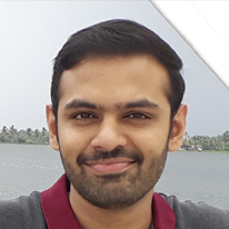 Dr. Jhnanesh Somayaji B received his Ph.D from National Institute of Technology Karnataka (NITK Surathkal) in 2018. He was a visiting scholar at Indian Institute of Science Bangalore during 2015-2016. Currently, he works for Advanced Nano-devices & Computational Research Lab as a Project Associate at Department of Electronic systems Engineering, Indian Institute of Science, Bangalore. His research interests include Power semiconductors and circuits, submicron devices and technology. He is very passionate about music who can sing and play some of the well known percussion instruments.
Visit: http://msdlab.dese.iisc.ac.in/dr-jhnanesh-somayaji-b/
Monishmurali M
 Monishmurali M is from Bangalore. Did his schooling and graduation from Bangalore. He has a bachelors degree in Electrical engineering from PESIT, Bangalore. He is currently pursuing his PhD(From 2018 August) at Indian Institute of Science under the supervision of Prof. Mayank Shrivastava. His work focuses on ESD and Latch-up in non-planar CMOS nodes.
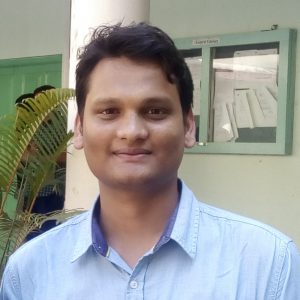 Om Kesharwani was born in Allahabad, India. He did his schooling from Anglo Bengali Inter college Allahabad, India. He pursued his B.Tech in Electrical and Electronics Engg. from NIT Arunachal Pradesh in 2017. He is a recipient of J.C. Bose Gold Medal for best project in undergraduate programmes. During his undergraduate he had worked on high efficiency tandem solar cell at Center for Nano science & Engineering (CeNSE), Indian Institute of Science Bangalore. He is currently pursuing his PhD at Indian Institute of Science under the supervision of Prof. Mayank Shrivastava. His work focus on the design of High Voltage Silicon power devices in Non-planar CMOS technology. He likes exploring the new place, playing cricket volleyball and tennis, enjoy cooking and is a cinephile.
Visit :http://msdlab.dese.iisc.ac.in/Omkesharwani/
 Kranthi Nagothu is from the state of Andhra Pradesh, India. He obtained his B.Tech degree from Jawaharlal Nehru Technological University, Kakinada in 2012 and M.tech from National Institute of Technology Calicut, Kerala in 2014. He was with ST Micro Electronics, Noida as a graduate trainee from June, 2013 to July, 2014. Later he joined ANDCRG, DESE, IISc, as a research assistant. Currently he is pursuing his Ph.D from the same group. His research interests include exploration of Electro Static Discharge (ESD) behaviour of beyond CMOS technologies (Tunnel FETs and Graphene FETs) and power scalability issues in advanced High Voltage CMOS technologies specific to Silicon Controlled Rectifiers (SCR) in Laterally Double diffused MOS (LDMOS) Devices. He likes to keep himself updated with the current affairs and enjoys playing cricket and cycling. To know more about research pubilcations Visit: http://msdlab.dese.iisc.ac.in/kranthi-nagothu/
 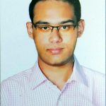 Rajarshi Roy Chaudhuri hails from Kolkata, West Bengal. He did his schooling in Kolkata and went on to receive the B.Tech. degree in Electronics and Communication Engineering from the West Bengal University of Technology, India in 2016. He then pursued his M.Tech degree in Electronics and Telecommunication Engineering from the Indian Institute of Engineering Science and Technology (IIEST), Shibpur, India during 2016-2018. He is currently in the first year of his Ph.D., which he is pursuing since 2018, in the MSD Lab, Department of Electronic Systems Engineering, Indian Institute of Science (IISc), Bengaluru.
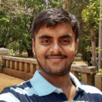 Rajat pursued his B.E in Electrical and Electronics Engineering from Birla Institute of Technology, Mesra in 2015 and has since then moved to Bangalore to pursue his doctoral studies at IISc Bangalore under the supervision of Prof. Mayank Shrivastava and Prof. Sanjiv Sambandan. His work focusses on understanding the Electrostatic Discharge behavior of flexible electronic devices with a focus on existing a-Si: H technology and futuristic technologies including Organic electronics and Metal oxides based semiconductor technology. His work is aimed at understanding the physics of device failure and degradation, electro-thermal charge transport and material specific high field high-frequency effects with an aim of aiding technology development in these areas.In his spare time, he likes to read and explore different places. Visit:http://msdlab.dese.iisc.ac.in/rajat-sinha/
.
Industry Volunteers
If you wish to become a volunteer please write to indiaesdfourm@gmail.com
