1st India ESD Workshop (2016)
Venue: Department of ESE, Indian Institute of Science (IISc) Bangalore
Date: Feb 16th 2016
Hosted, organized and envisioned by: Prof. Mayank Shrivastava, Indian Institute of Science Bangalore
Highlights and Summary: With the vision to strengthen and promote ESD activities in India the concept of “India ESD Forum” was first envisioned in 2015. The idea behind this vision was three fold. First, is to increase ESD awareness among engineers and academicians working in the field of VLSI / Microelectronics and provide opportunity to local engineers who would like to learn or engage into ESD protection device/circuit/product design and testing activities. Second, to bring together engineers who often encounter ESD design problems. Third, to encourage research, development and training related to on-chip ESD protection device/circuit design in India. Within 2 months this forum has attracted registration from 63 senior level engineers and technical managers working in a number of VLSI design companies (Fig. 1) in India. This gives encouraging hope to organize and eventually bring together under one roof all of the VLSI engineers in India, and in due course engineers in the South East Asia, interested in ESD activities.
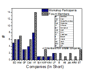
Figure 1: Company wise distribution of workshop participants and forum members.
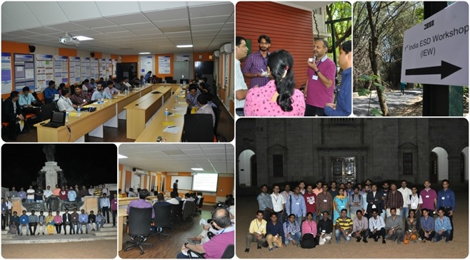
Figure 2: Visuals from the 1st India ESD Workshop.
Given the great interest shown by VLSI professionals, 1st India ESD Workshop (IEW) was envisioned, organized and hosted by Prof. Mayank Shrivastava. The workshop received an excellent response from the VLSI community. 33 industry professionals from semiconductor technology giants like SanDisk, Intel, Global Foundry, NXP, Cadence, Infineon and Synopsys joined this workshop along with 7 students and 3 faculty members (Fig. 2). Without any exaggeration this can be called a good start. The attendees participated in a highly engrossing manner with in depth technical discussions and sessions. Technical discussions were later complemented by ESD experts Dr. Harald Gossner and Dr. Charvaka Duvvury, through teleconferencing during a session called “Ask the Experts”. Later the host together with the participants laid down strategy and roadmap for the forum and future workshops.
By and large the workshop was found to be highly valuable for the VLSI community in India and therefore similar workshops one in every 4 months were unanimously requested by the participants. Considering the enthusiasm of the participants towards this new initiative and willingness to contribute, an expected participation of 100 VLSI professionals, faculties and students in the next workshop would not be farfetched. More importantly, the next workshops will be planned to have contributed talks from the participants leading to a fully fledged 2 day event within 1.5 years addressing VLSI community in the South East Asia
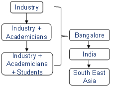
Figure 3: Roadmap and vision for India ESD forum and workshop
Questions & Concerns – Technical Discussion:
- Does custom ESD design ensure better ESD robustness?
- How the designers can ensure that given ESD guidelines are the best?
- Where are these design guidelines coming from? Why the guidelines are not elaborated enough, i.e. why only numbers, why not justification and physical explanation too?
- There is a serious need to improve understanding from technology side. The gap is increasing with each technology node.
- As an I/O designer we are often have to live with some black box ESD guidelines and we are asked to qualify our designs for a given standard. Is there a better way of doing ESD design? How difficult it is to do ESD simulations?
- There is a serious gap between academia and industry, which is required to be bridged.
- Similarly there is also a gap between the ESD experts and circuit designers, which is required to be bridged. Training from both the sides is required.
- Many designers expressed interest in tools and models for ESD simulations; however it was concluded that doing realistic ESD simulations is extremely challenging and requires strong industry and academia collaboration.
- Few designers asked whether it is possible to get same or better ESD robustness for high performance chips while sacrificing less Si real estate.
- Several designers suggested that a course on ESD design should be included in the post graduate curriculum.
- The End users of ICs and system designers, especially in this region have very little knowledge of ESD! There is a need to bridge the gap.
- Shouldn’t there new system level ESD standards for Indian conditions?
- How do the biomedical devices handle ESD given that these devices are directly in contact with human body?
- The device designers also don’t clearly know what the circuit designers want!
- Gap between the Foundry and circuit designer should be addressed. A few ESD groups do device – circuit co-design up to a certain extent. But it’s not possible for fabless companies. Designers need technology training for better understanding.
- How to handle ESD robustness specs desired by different IP customers? Often different customers ask for different robustness levels for the same IP with different ESD protection strategies for inter IP protection. How this situation should be handled.
- Are ESD protection strategies application driven, or driven by IP design requirements?
- It became difficult to find the root cause for failure at the system level, any simulation strategies available for the same?
- If factories can improve their environment and make it ESD robust, can we get rid of ESD protection?
- Can a fabless company have their own ESD library to bridge the gap between foundry and designers? In this case how to strengthen the fabless companies?
- How to bridge the gap between on chip ESD designers and system level designers?
- How to make FinFET devices ESD robust, what are various future challenges in this technology?
- Often the ESD cells are more complex than the normal functional cells. Its 3x harder to handle ESD cell. Can this forum offer trainings to make designers life easier? Are the ESD cells over designed? Are we doing more than what is required?
- What is the definition of ESD expert? Who can be called an ESD expert? Is Ph.D, a must to become an ESD expert?
- Technical Discussion: on the basics of ESD, difficulty in system level ESD than in on-chip level ESD.
- What is the right time to worry about ESD in emerging devices and technology?
- The know-how regarding the ESD constraints, rules and regulations should be expanded, and the gap between the ESD reliability designers and the circuit designers should be bridged.
Questions & Concerns – Ask the Expert:
- The ESD design guidelines are provided by the foundry. Can we modify these guidelines by some small margins? How to reduce the size of the devices given in the guidelines still meeting the standards?
- Despite following the rules from the foundry have you ever encountered a failure?
- Is there any standard if device doesn’t turn on during an ESD event. What one should do to ensure that there is no damage, even if this happens?
- What happens if there is an ESD discharge during the above mentioned condition?
- What role metal and bond wire inductors play under CDM like ESD causing the failures. Is there any EDA tool which can model this?
- FinFET devices have more latch up concerns and we were asked to keep substrate contacts closer. Can you elaborate on this?
- If we increase the off chip ESD protection, can we relax the on chip ESD protection?
- IC4-2, the displays are failing due to magnetic field. We are unable to get proper data for magnetic field probing? Can you suggest something on this?
Technical Discussion & Questions:
- How can one ensure false triggering of ESD clamps during normal IC operations to be absent?
- How to address the ESD issues in FinFET technologies?
- Can we model the variation in ESD robustness for different PVT conditions?
- There is serious concern and need to bridge the gap between designer and the foundry. Is it practically possible to bridge the gap given the competition among various companies?
- How much knowledge is available for the futuristic ESD devices in the public domain?
- Circuit level and system level understanding is missing by and large.
- In cross domain CDM protection where the grounds of the two domains are isolated even in package what is the confidence that, the chip would be immune to CDM event? How do I decide the optimum CDM ESD protection with best interest of capacitance load, timings, silicon real-estate?
- Derivation of simplified model for the ESD cells and how to arrive at the cell parameters in order to reduce the over designs.
- Would like to know robust test structures and post silicon testability conditions and solutions for faster convergence debug.
- Would like to have knowledge on pin capacitance reduction, device guidelines, ESD modeling at different levels, power ESD?
- Would like to see more and more signal friendly ESD practices.
- Basic training on devices and their interaction with circuit level.
- Approach to bridge the gap between system level ESD and on chip ESD protection?
- As a circuit and layout designer I have no idea of system level ESD protection. Can this forum and workshop help in this?
- Would like to know the know-how in Advanced ESD protection and FinFET technologies.
- On chip vs. off chip ESD requirements and relations between the two.
- Leakage reduction in lower technology nodes while not compromising on ESD events.
- Need more details on why gate cannot be connected to supply/ground, when the same is fine for decoupling capacitors? Why is it fine for CDM clamps and not for functional devices?
- Role of decoupling capacitors on supply pins in terms of providing ESD protection?
- How to handle ESD protection for RF pins which have requirements of < 50 pF of capacitive loading?
- Need to strengthen device modeling to perform IP level ESD simulations.
- A session focusing on basics of ESD design to understand fundamentals/terminology of ESD/EOS for beginners.
- For full chip ESD simulations (which are very complicated in nature) what kind of efforts are needed from the foundry or at the modeling front?
- From IC design point of view, what is the best time to take care of ESD concerns?
- What are the on-chip ESD protection requirements to ensure better system level ESD protection? In other words how on-chip ESD is correlated with system level ESD?
- As the root cause for ESD failures at system level are becoming more and more difficult to identify. Proper failure analysis methodologies at system level and extensive verification through simulations are required to be addressed.
Suggestions:
- Industry should find ways to increase academia-industry tie-ups in the near future for upcoming technologies. This is one way to bridge the gap and improve the knowhow of engineers.
- Case studies are often very important and this should be one of the focus area for the planned 2 day events and contributed talks.
- This focus and workshop should offer a medium to share and discuss the common ESD failure problems.
- All new activities in the forum should be shared to the members.
- Regular sessions on various aspects of ESD protections with focused technical discussions.
- Include problems/ solutions from various designers and discuss them in technical sessions.
- Technical paper presentations from companies can be included.
- Regular training on selected topics, case studies, some set of presentations with brain storming sessions.
- Can we have different members of the forum contributing to the training?
- Ways to reduce the gap between ESD designers and core circuit designers.
- Verification of ESD at IC level as well as system level.
- ESD is a topic with very less awareness in the academia and even in industry. We need to market this forum better. Like popular magazines, social media, various communities. This will help in generating interest and experts in the industry and among students.
- Collaborating with other ESD communities across the globe would be great.
- This forum should encourage master’s students by giving required knowledge on ESD.
- This workshop should emerge as a EOSESD symposium like conference with paid training.
- Two day conference with general sessions and training sessions by industry experts.
- Frequent workshops (3 per year) would be nice.
- Forum should come up with proceedings every year with system level and chip level ESD issues and solutions.
- Forum should create more ESD awareness among the end users. It would be good to prepare a tutorial on ESD and publish in prominent magazines.
Feedback:
- Conducting workshop in morning session or Saturdays.
- Good start towards looking at ESD problems and solutions with today’s challenges.
- Appreciate interactive talk with Herald Gosner and Charuvaka.
- Looking forward to next workshops of IEW.
- Conducting in other cities in INDIA and inviting customers and designers.
- Advanced design can be discussed.
- Tutorial workshops on fundamentals (ESD,EOS,Latch-up) before delivering high-end problems.
- Discussion of technical papers.
- Monthly WEBEX for working group. Quarterly face to face meeting. Expert will be presenting on single topic while others contribute by providing short presentations.
- Any books or papers.
- Include Hands-on, more challenging problems, case study, mix device physics, lesser statistics.
- Include less technical more on challenges being faced